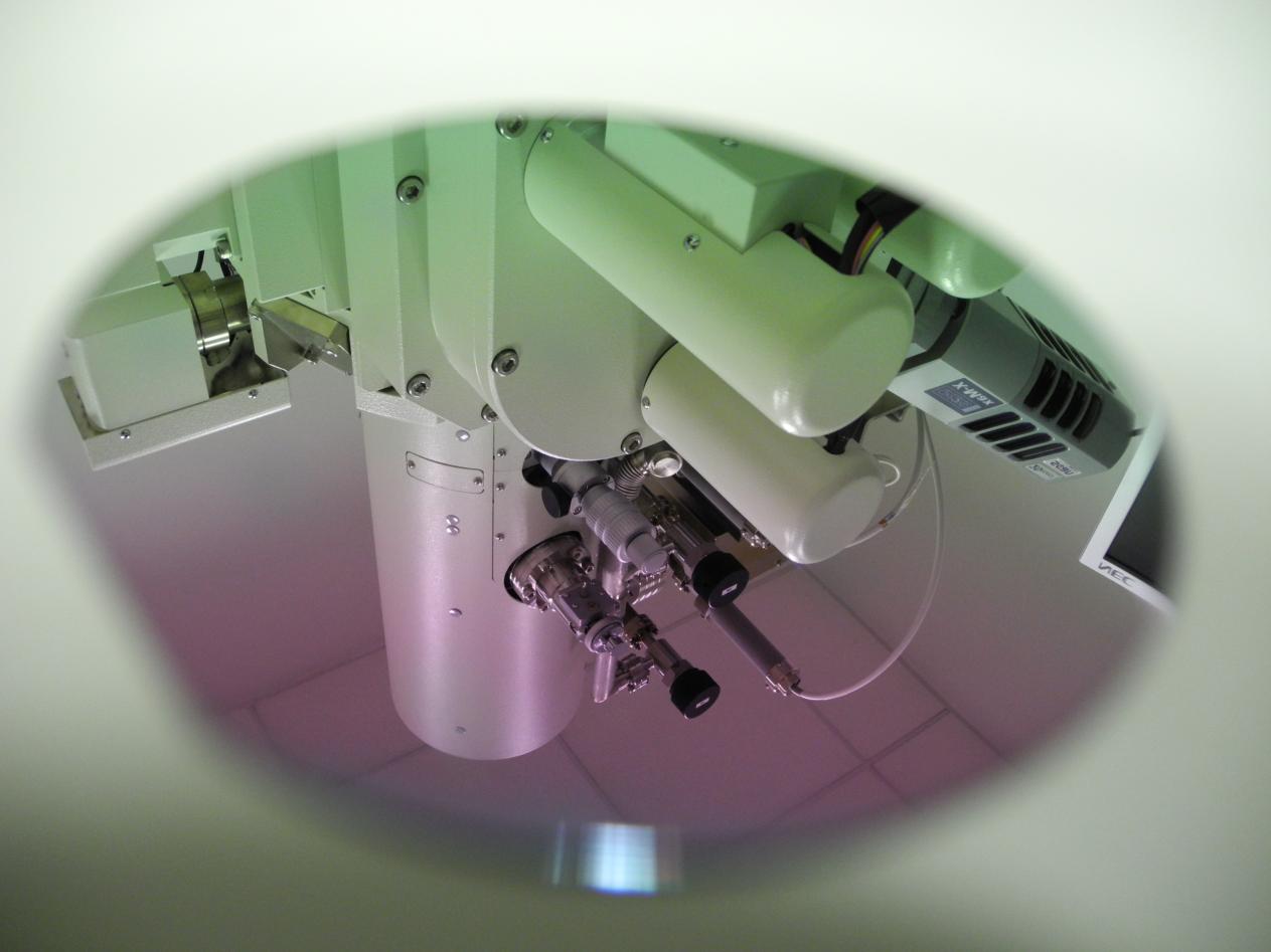
EBL - Electron beam lithography

System:
Field size, usual applications:
200 microns
Stage accuracy:
+- 2.5 microns
Pattern design:
Exposure Control Program (ECP) - software for pattern design and exposure with the XENOS pattern generator. Structure and its layout are defined in special control file (ctl), which is a composition of several patterns. Patterns consist of primitive shapes (dots, lines, rectangles, circles). Control file also includes parameters of exposure; exposure time, beam current, rasterization (increment), other options (field size, dscale,...).
Substrate:
Typically silicon wafer with a thin layer of oxide on top.
Resist:
PMMA 950K 2%-5%, (for double layer) PMMA/MA 33% (Allresist Gmbh.), coating: spinner: 2000-6000rpm/min; baking 180°C for 10 min on a hot plate
Tipcal drawing parameters:
acceleration voltage: 10 - 25 kV; beam current: 50 - 1000 pA
Developer:
mixture (methyl-isobutyl-ketone) MIBK: (isopropanol)IPA = 1:3, 1 min
Stopper:
IPA, 1 min
Metal deposition:
sputtering, PECS Gatan Inc.
Lift-off:
acetone, at least 2 hours at 45°C