Nanolithography - Basic procedure

The basic procedure of nanolithography does not depend on the system (e-beam or laser), and it can be shortly summarized in seven steps. However the pattern transfer onto the substrate can be achieved in different ways and thus the process of nanolithography may differ form the scheme described below.
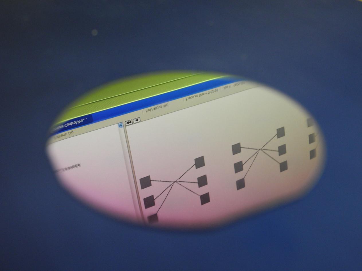
Designing the pattern
The pattern is designed with appropriate software, which depend on the system. Often a CAD file format is used, which incorporates specified primitive shapes (lines, rectangles, dots,...), their position and parameters that influence the dose.
Preparation of the substrate
For good resist adhesion and high resolution of features, the cleanliness of substrate is very important. Several cleaning methods are possible to use within the preparation of the substrate if necessary: ultrasonic bath in acetone or some other solvent, plasma etching, pre-coating with some activation medium and similar. Different materials can be used for substrates. E-beam lithography requires the substrates to be conductive. If we still want to use nonconductive material than the dissipation of the charge must be provided e.g by additional conductive coating.
Resist spin-coating
Resist is a transfer media for nanolithography. The coating is made by dropping the liquid resist onto the substrate and spinning it. The thickness of the layer can be controlled with revolution speed of the spinning. Afterwards the resist must be baked for some time, for solvent to evaporate and film to solidify. Usually air conditions (temperature, humidity) must be within some limits, since they influence the resist properties (e.g. sensitivity, contrast).
Illumination - drawing with the beam
This is the essential phase in the process of the nanolithography process. Machine system controls the beam movements precisely following the pattern specified in the control file. In machine code each segment of the structure is composed of dots, so every exposed area actually consist of beam spots. These are usually much wider than the beam diameter alone, since interacting area of the photons or electrons is much bigger. When resist is exposed by the beam structural modifications in polymer chain appear (the exact mechanism depends on the resist), so that in the next stage, the appropriate solvent can remove the damaged molecules in the beam trail.
Development
The substrate is dipped in the solution - developer, which dissolves the damaged resist in illuminated places. Development is finished with stopper (clean solvent of developer) washing away the developer and dissolved resist. Both processes typically take about a minute. Channels and holes in the residual resist forms the designed structure. For final pattern transfer it is important that channels are cleared of resist all the way down to the substrate surface. Development is finalized when the substrate is blown dray with compressed air or nitrogen.
Metal coating
Final pattern transfer starts with the deposition of chosen metal or some other solid material (carbon) onto the substrate, either with sputtering or chemical deposition. In the channels, which represents pattern, metal adheres directly to the substrate, while elsewhere the resist layer separates the metal from the substrate.
Lift-off
During the lift-off process residual resist is dissolved in a stronger solvent - remover (typically acetone). The overlaying metal cracks and comes off the substrate, leaving the metal structure only in the pattern areas (channels and holes) where the metal was deposited directly on the substrate.